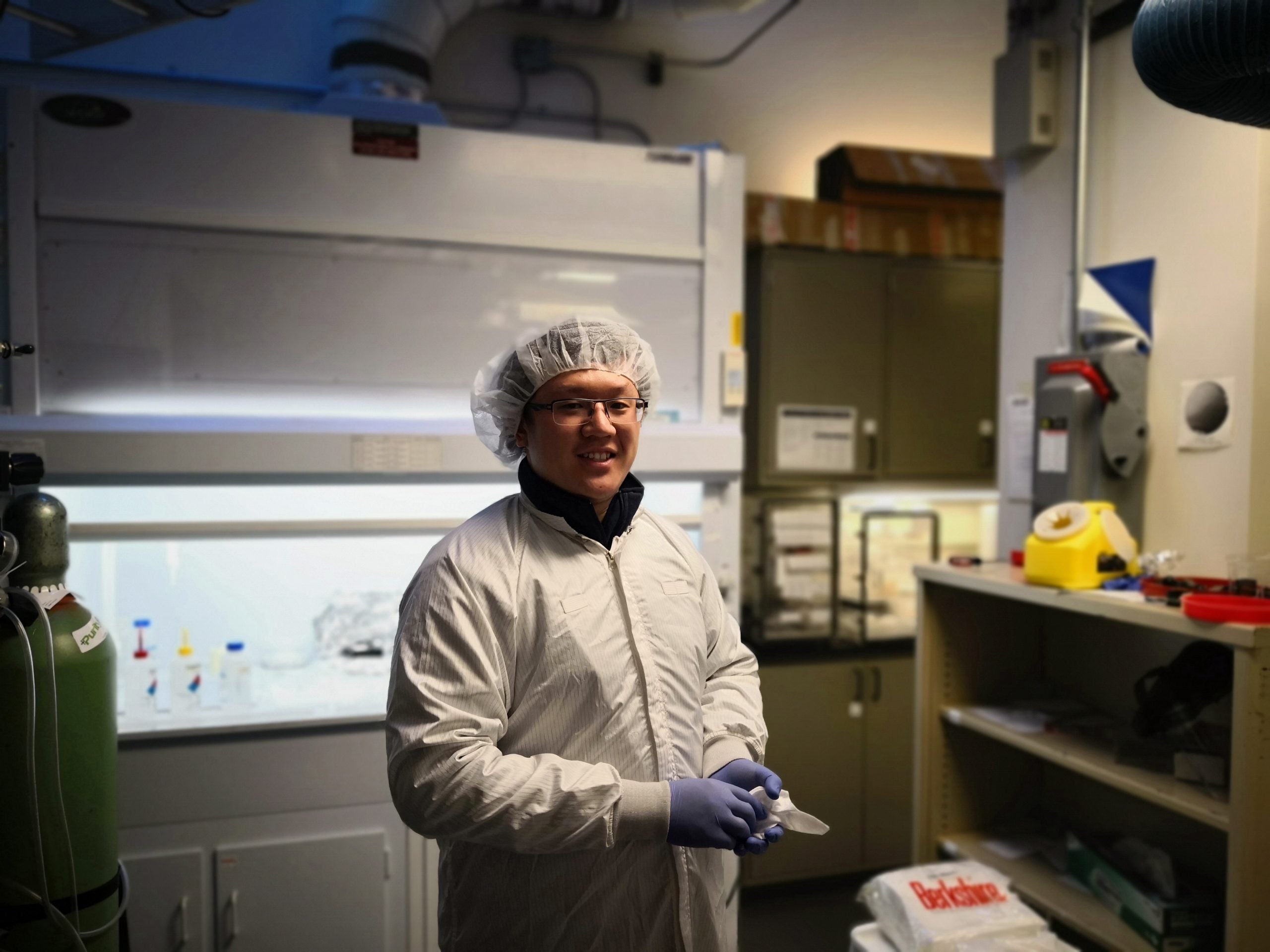
Jiaheng He

Pronouns: He/Him/His
UROP Fellowship: University of Michigan Energy Institute
Research Mentor(s): Rachel Goldman, PhD
College of Engineering, Department of Materials Science & Engineering
Presentation Date: Thursday, July 30, 2020 | Session 1 | Presenter: 2
Authors: Jiaheng He, Maggie Chen, Guanjie Cheng, Davide DelGaudio, Fabian Naab, Zishen Wang, Bin Li, Jung Han, and Rachel S. Goldman
Abstract
Although silicon-based electronics are used to power light-emitting diodes and electric vehicles, their utility in high power applications is limited by low breakdown voltages. The most promising alternatives are vertical GaN devices, but these involve etching and selective-area re-growth, both of which enhance near-surface atomic displacements to the detriment of device performance. In this work, we utilize ion beam analysis and cathodoluminescence spectroscopy to examine the influences of ambient exposure, dry etching, and metal-organic precursor surface treatments on surface/interface defects and their electronic signatures. First, we discuss the influence of ambient exposure and dry etching on the structure and properties of regrown p-i-n GaN structures. We demonstrate that dry etching improves the crystallinity of p-i interfaces, but also introduces interfacial hydrogen. We then describe our investigations of the influence of dry etching and metal-organic precursor surface treatments on the structure and properties of GaN substrates and overgrown GaN layers. To date, we have shown that the metal-organic precursor reduces surface atomic displacements, leading to high-intensity band-to-band cathodoluminescence emission following overgrowth. In addition to presenting these findings, we will discuss progress towards quantifying the concentration and distribution of displaced Ga and N atoms using a combination of two-dimensional ion channeling maps and ion channeling simulations.
Google Slide Presentation
Presentation Script
Research Disciplines
Engineering


